
8Bit Adder—SystemModeler Model
Explore the world of digital circuit design with our tutorial on implementing a Full Adder using an 8:1 MUX! Dive into Number Systems and Code, understanding.

Full 8bit adder
Compared to a conventional CMOS-based full adder, the power consumption was reduced by 13.78%. We also designed a low-power 8-bit signed multiplier based on the proposed full adder. The post-layout simulation showed an 8% power reduction compared to the multiplier produced by the DC synthesis tool.
csőd egészségtelen Bírság 4 bit full adder truth table javul Trunk könyvtár Trunk könyvtár
Download Full Model The 8-Bit Adder Principle The 8-bit adder adds the numbers digit by digit, as can be seen in the schematic diagram below. In this example, the integers 170 and 51 represent input a and b, respectively, and the resulting output is the sum 221.
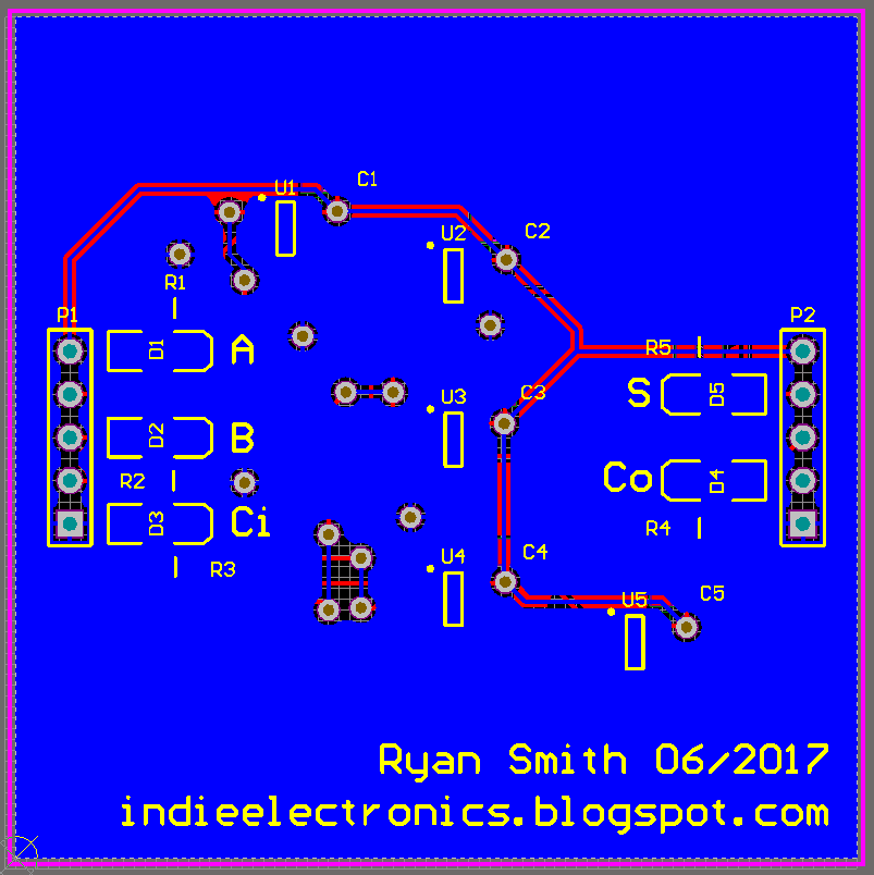
Indie Electronics My 1 Bit Full Adder Project
Design a 8-bit carry-ripple adder with any circuit family. Verify it and report the performance of your design, including delay, EDP, area(# of transistors) LAB Requirements. Optional part: Tasks. Design your full adder with other circuit families and compare the performance metric EDP by the possible methods: Insert the buffers to optimize the.

4 bit binary substractor Schema Digital
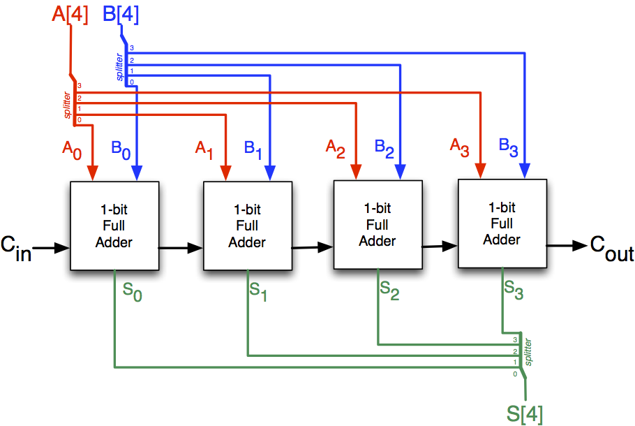
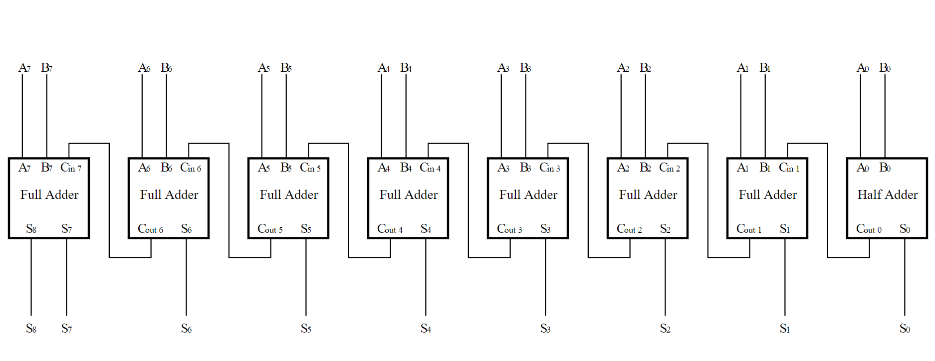
The 8bit Adder is comprised of eight Full Adders which are connected by their carry in/out. The Full Adder gives the sum of two, 1-bit inputs. Likewise the 8 bit Adder gives the sum of two 8-bit inputs. This 8-bit Adder starts at the top left corner and is finished at the bottom right.
Half Adders & Full Adders A Level Computer Science
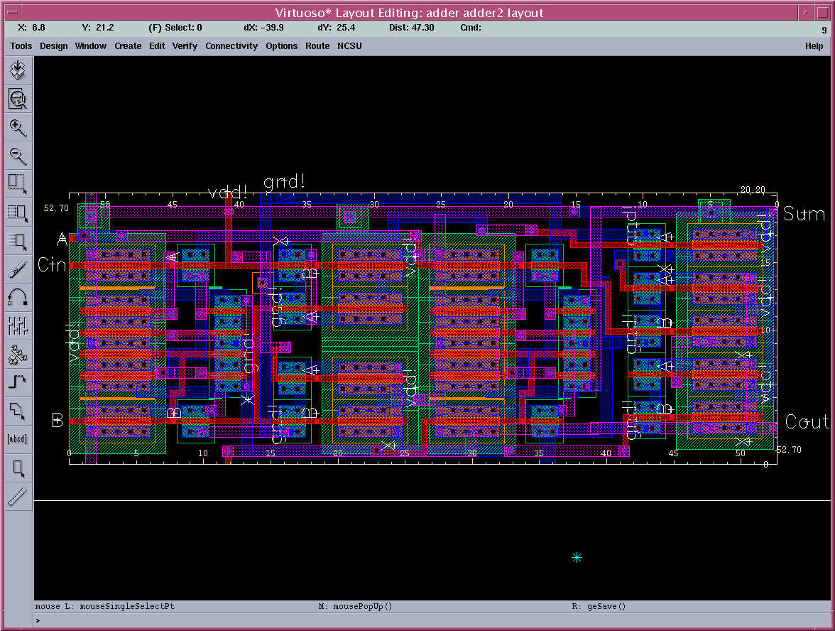
8-bit adder (For Grad Student only): 8-bit adder is the composition of eight 1-bit adder. So when you copied all the 1-bit adder side by side you will get the 8-bit adder. Figure 6: Schematic of 8-bit full Adder in cadence To get the layout of 8-bit adder you need to add the layout of 1-bit adder side by side. So
8 Bit Adder Circuit
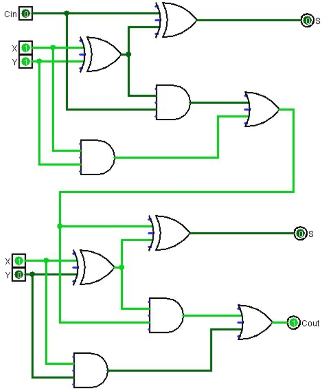
8 Bit Adder Description of Parts: A full adder is a combinational circuit that forms the arithmetic sum of three input bits. It has two inputs: X and Y, that represent the two significant bits to be added, and a Z input that is a carry-in from the previous significant position.
[CRACKED] 8bitfulladder
A full adder logic is designed in such a manner that can take eight inputs together to create a byte-wide adder and cascade the carry bit from one adder to another. we use a full adder because when a carry-in bit is available, another 1-bit adder must be used since a 1-bit half-adder does not take a carry-in bit.

Full Adder Circuit 4 Bit
Step 3: Full Adder. Using 3 digital logic gates (AND, OR, and XOR), we can create what is known as a Full Adder circuit. A full adder takes in 3 inputs. A carry and two binary inputs. An adder is meant to 'add' two binary inputs. If A and B are both 0 (LOW signals), the output will be 0, assuming there is no carry.

Introduction to Full Adder projectiot123 esp32,raspberry pi,iot projects
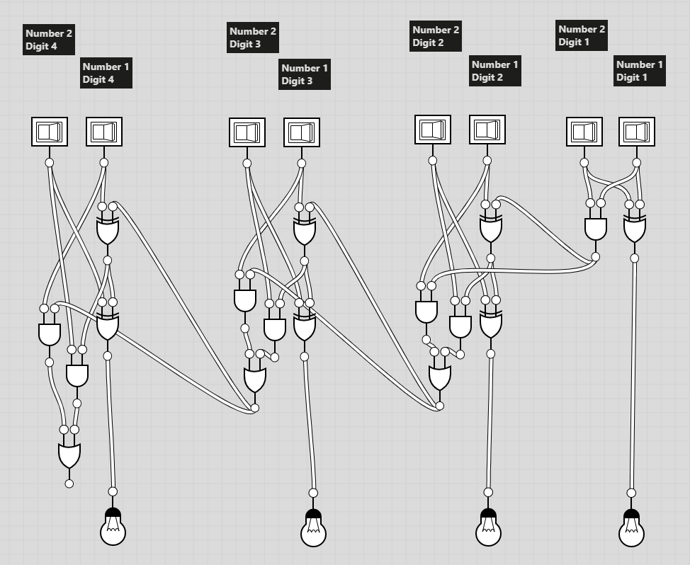
These full adders can also can be expanded to any number of bits space allows. As an example, here's how to do an 8 bit adder. This is the same result as using the two 2-bit adders to make a 4-bit adder and then using two 4-bit adders to make an 8-bit adder or re-duplicating ladder logic and updating the numbers.
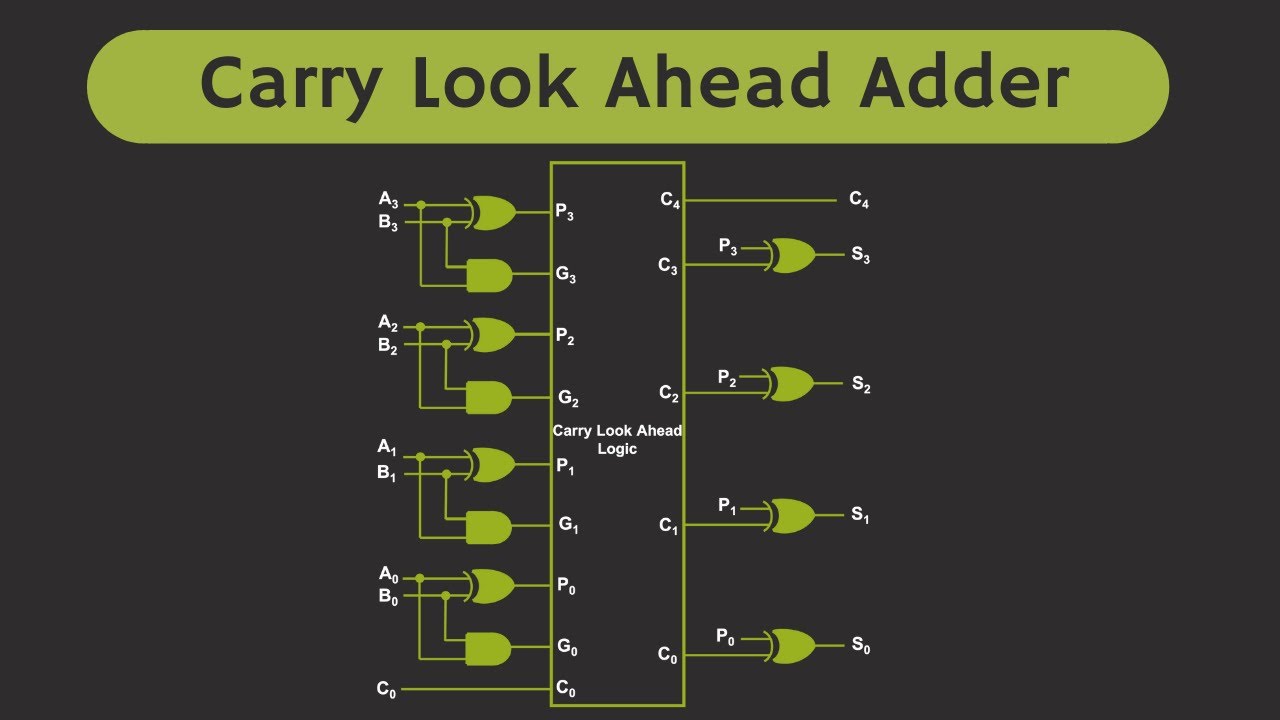
4 Bit Carry Look Ahead Adder Circuit Diagram
11 11 11 --- 110 Look at how many inputs the middle column uses. Our adder needs three inputs; a, b, and the carry from the previous sum, and we can use our two-input adder to build a three input adder. Σ is the easy part. Normal arithmetic tells us that if Σ = a + b + C in and Σ 1 = a + b, then Σ = Σ 1 + C in. What do we do with C 1 and C 2?
CS 3410 Spring 2018 Lab 1
An Adder is a digital logic circuit in electronics that performs the operation of additions of two number. Adders are classified into two types: half adder and full adder. The full adder (FA) circuit has three inputs: A, B and Cin, which add three input binary digits and generate two binary outputs i.e. carry and sum. Contents show Truth. title="Full Adder - Truth table & Logic Diagram.

Trouble Designing an Adder that works with register in Logisim Electronics and Electrical
A Full Adder can be built using two Half Adders circuits and an OR gate. The first Half Adder has two 1-bit binary inputs, which are A and B. It produces two outputs; Sum and Carry. The Sum output of the first Half Adder will be the first input of the second Half Adder. And the Carry output of the first Half Adder will be the second input to.
Half Adders & Full Adders A Level Computer Science
Learn how to implement a 8-bit Full Adder in Verilog.GITHUB: https://github.com/kirkster96/VerilogTutorialsPlaylist: https://www.youtube.com/playlist?list=PL.

Trudiogmor 8 Bit Full Adder Truth Table
entity FA_8bit is port (x,y : in std_logic_vector (7 downto 0); cin : in std_logic; sum : out std_logic_vector (7 downto 0); co : out std_logic); end FA_8bit; architecture FA_arch of FA_8bit is signal cary : std_logic_vector (6 downto 0); component full_adder is port (p,q,r:in std_logic; sm,cr: out std_logic); end component; begin
8 bit full adder
8 Bit Full Adder Circuitlab Ripple Carry Adder Types Workin Advantages And Its Applications Implementation Test Pattern Generation And Comparative Analysis Of Diffe Adder Circuits Full Adder Combinational Logic Functions Electronics Textbook